Press release
Growth of Wafer Surface Defect Detection Equipment Market, Revenue, Manufacturers Income, Sales, Market Trend Report Archives in 2024

The global Wafer Surface Defect Detection Equipment market was valued at US$ million in 2023 and is anticipated to reach US$ million by 2030, witnessing a CAGR of %during the forecast period 2024-2030.
【Get a free sample PDF of this report (Including Full TOC, List of Tables & Figures, Chart)】
https://www.qyresearch.com/reports/3133033/wafer-surface-defect-detection-equipment
Wafer surface defect detection equipment refers to advanced inspection tools and systems designed to identify and analyze imperfections or irregularities on the surface of semiconductor wafers. These defects can include scratches, pits, particles, and pattern deviations, which can adversely affect the performance and yield of semiconductor devices. The primary goal of this equipment is to ensure the quality and reliability of wafers used in the production of integrated circuits (ICs) and other semiconductor components.
According to the new market research report "Wafer Surface Defect Detection Equipment- Global Market Share and Ranking, Overall Sales and Demand Forecast 2024-2030", published by QYResearch, the global Wafer Surface Defect Detection Equipment market size is projected to reach USD 2.14 billion by 2030, at a CAGR of 6.3% during the forecast period.
According to QYResearch Top Players Research Center, the global key manufacturers of Wafer Surface Defect Detection Equipment include Nordson, Hitachi High-Tech, Skyverse, KLA, ISRA VISION AG, Tokyo Electron Device, Cognex, TSI, Dark Field Technologies, ZC Optoelectronic, etc. In 2023, the global top five players had a share approximately 59.0% in terms of revenue.
Market Drivers:
The growing use of semiconductor devices in various applications such as consumer electronics, automotive, telecommunications, and industrial sectors drives the need for high-quality wafers, boosting the demand for defect detection equipment.
As semiconductor technology advances, including the development of smaller nodes and more complex architectures, the need for precise defect detection becomes more critical, driving the market for advanced detection equipment.
Restraint:
The high cost of advanced wafer surface defect detection equipment can be a significant barrier, particularly for small and medium-sized enterprises.
The complexity of operating and maintaining defect detection equipment requires skilled personnel, which can be a limitation for some manufacturers.
Trends:
The integration of artificial intelligence (AI) and machine learning algorithms in defect detection systems is a growing trend. These technologies enhance the accuracy and speed of defect identification and classification.
Increasing automation in semiconductor manufacturing processes, including defect detection, is driving the development of automated inspection systems that can operate with minimal human intervention
The report provides a detailed analysis of the market size, growth potential, and key trends for each segment. Through detailed analysis, industry players can identify profit opportunities, develop strategies for specific customer segments, and allocate resources effectively.
The Wafer Surface Defect Detection Equipment market is segmented as below:
By Company
AMETEK
Nordson
Vitronic GmbH
Omron
IMS Messsysteme GmbH
ISRA VISION AG
Synergx
Perceptron
Inovision
Dark Field Technologies
Hitachi High-Tech
Baumer Inspection
Icemi
AUTIS Engineering
Segment by Type
Based on Image Processing
Based on NDT
Segment by Application
Semiconductor Wafer Inspection
Semiconductor Mask/Film Inspection
Each chapter of the report provides detailed information for readers to further understand the Wafer Surface Defect Detection Equipment market:
Chapter 1: Introduces the report scope of the Wafer Surface Defect Detection Equipment report, global total market size (valve, volume and price). This chapter also provides the market dynamics, latest developments of the market, the driving factors and restrictive factors of the market, the challenges and risks faced by manufacturers in the industry, and the analysis of relevant policies in the industry. (2019-2030)
Chapter 2: Detailed analysis of Wafer Surface Defect Detection Equipment manufacturers competitive landscape, price, sales and revenue market share, latest development plan, merger, and acquisition information, etc. (2019-2024)
Chapter 3: Provides the analysis of various Wafer Surface Defect Detection Equipment market segments by Type, covering the market size and development potential of each market segment, to help readers find the blue ocean market in different market segments. (2019-2030)
Chapter 4: Provides the analysis of various market segments by Application, covering the market size and development potential of each market segment, to help readers find the blue ocean market in different downstream markets.(2019-2030)
Chapter 5: Sales, revenue of Wafer Surface Defect Detection Equipment in regional level. It provides a quantitative analysis of the market size and development potential of each region and introduces the market development, future development prospects, market space, and market size of each country in the world..(2019-2030)
Chapter 6: Sales, revenue of Wafer Surface Defect Detection Equipment in country level. It provides sigmate data by Type, and by Application for each country/region.(2019-2030)
Chapter 7: Provides profiles of key players, introducing the basic situation of the main companies in the market in detail, including product sales, revenue, price, gross margin, product introduction, recent development, etc. (2019-2024)
Chapter 8: Analysis of industrial chain, including the upstream and downstream of the industry.
Chapter 9: Conclusion.
Benefits of purchasing QYResearch report:
Competitive Analysis: QYResearch provides in-depth Wafer Surface Defect Detection Equipment competitive analysis, including information on key company profiles, new entrants, acquisitions, mergers, large market shear, opportunities, and challenges. These analyses provide clients with a comprehensive understanding of market conditions and competitive dynamics, enabling them to develop effective market strategies and maintain their competitive edge.
Industry Analysis: QYResearch provides Wafer Surface Defect Detection Equipment comprehensive industry data and trend analysis, including raw material analysis, market application analysis, product type analysis, market demand analysis, market supply analysis, downstream market analysis, and supply chain analysis.
and trend analysis. These analyses help clients understand the direction of industry development and make informed business decisions.
Market Size: QYResearch provides Wafer Surface Defect Detection Equipment market size analysis, including capacity, production, sales, production value, price, cost, and profit analysis. This data helps clients understand market size and development potential, and is an important reference for business development.
Other relevant reports of QYResearch:
Wafer Surface Defect Detection Equipment- Global Market Share and Ranking, Overall Sales and Demand Forecast 2024-2030
Global and United States Wafer Surface Defect Detection Equipment Market Report & Forecast 2024-2030
Global Wafer Surface Defect Detection Equipment Market Insights, Forecast to 2030
If you have any queries regarding this report or if you would like further information, please contact us:
QY Research Inc.
Add: 17890 Castleton Street Suite 369 City of Industry CA 91748 United States
E-mail: global@qyresearch.com
Tel: 001-626-842-1666(US) 0086-133 1872 9947(CN)
EN: https://www.qyresearch.com
JP: https://www.qyresearch.co.jp
QYResearch founded in California, USA in 2007.It is a leading global market research and consulting company. With over 17 years' experience and professional research team in various cities over the world QY Research focuses on management consulting, database and seminar services, IPO consulting, industry chain research and customized research to help our clients in providing non-linear revenue model and make them successful. We are globally recognized for our expansive portfolio of services, good corporate citizenship, and our strong commitment to sustainability. Up to now, we have cooperated with more than 60,000 clients across five continents. Let's work closely with you and build a bold and better future.
QYResearch is a world-renowned large-scale consulting company. The industry covers various high-tech industry chain market segments, spanning the semiconductor industry chain (semiconductor equipment and parts, semiconductor materials, ICs, Foundry, packaging and testing, discrete devices, sensors, optoelectronic devices), photovoltaic industry chain (equipment, cells, modules, auxiliary material brackets, inverters, power station terminals), new energy automobile industry chain (batteries and materials, auto parts, batteries, motors, electronic control, automotive semiconductors, etc.), communication industry chain (communication system equipment, terminal equipment, electronic components, RF front-end, optical modules, 4G/5G/6G, broadband, IoT, digital economy, AI), advanced materials industry Chain (metal materials, polymer materials, ceramic materials, nano materials, etc.), machinery manufacturing industry chain (CNC machine tools, construction machinery, electrical machinery, 3C automation, industrial robots, lasers, industrial control, drones), food, beverages and pharmaceuticals, medical equipment, agriculture, etc.
This release was published on openPR.
Permanent link to this press release:
Copy
Please set a link in the press area of your homepage to this press release on openPR. openPR disclaims liability for any content contained in this release.
You can edit or delete your press release Growth of Wafer Surface Defect Detection Equipment Market, Revenue, Manufacturers Income, Sales, Market Trend Report Archives in 2024 here
News-ID: 3671836 • Views: …
More Releases from QY Research
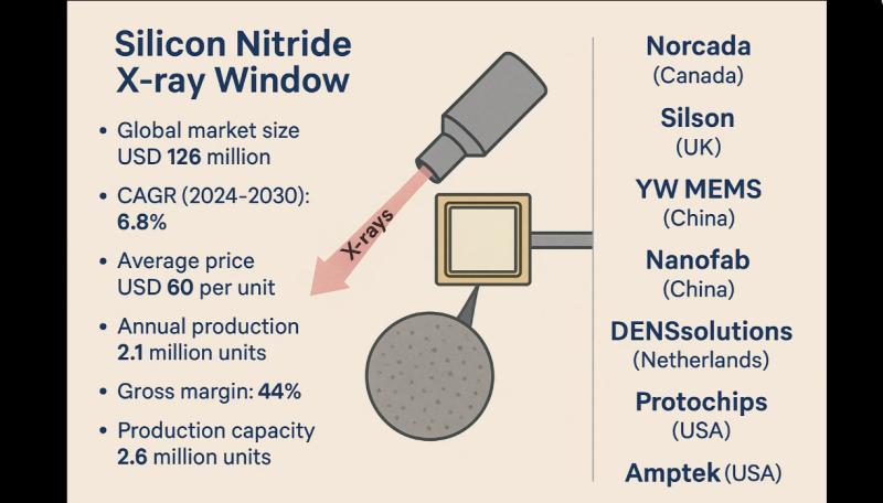
Global and U.S. Silicon Nitride X-ray Window Market Report, Published by QY Rese …
Intertek, a materials analysis company in the United States experienced repeated failures of thin-film X-ray detector windows made from polymer and beryllium due to mechanical fragility and poor chemical resistance. The breakage during high-vacuum operation caused costly downtime and contamination of sensitive detectors. To solve this, the company adopted Silicon Nitride X-ray Windows, fabricated using low-stress LPCVD Si3N4 membranes that combine extreme mechanical strength, chemical inertness, and high X-ray transmittance…
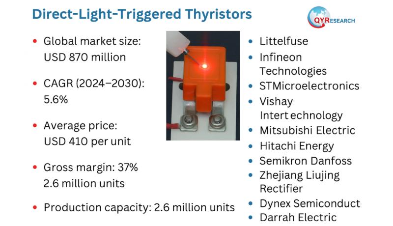
Global and U.S. Direct-Light-Triggered Thyristors Market Report, Published by QY …
A high-voltage DC transmission (HVDC) operator in Germany encountered reliability issues and signal latency in converter stations using electrically triggered thyristors. The traditional gate-drive circuits required complex insulation systems and additional control wiring, which increased electromagnetic interference (EMI) and maintenance costs. To overcome these limitations, the company adopted Direct-Light-Triggered Thyristors (LTTs) - power semiconductor devices that use optical fibers to trigger the thyristor directly via laser light, eliminating the need…
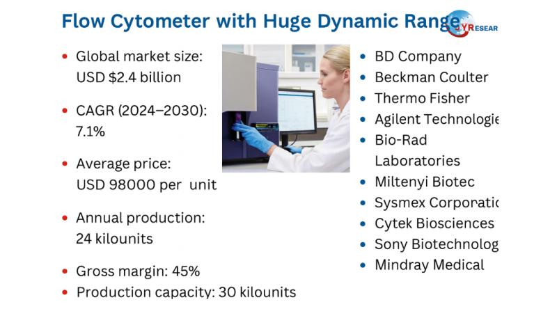
Global and U.S. Flow Cytometer with Huge Dynamic Range Market Report, Published …
A biomedical research institute in the United States faced major limitations in analyzing mixed-cell populations with traditional flow cytometers. Standard instruments suffered from signal saturation when detecting both dim and highly fluorescent cells simultaneously, resulting in poor quantification accuracy and repeated sample runs. To solve this, the lab upgraded to Flow Cytometers with Huge Dynamic Range, featuring advanced photon detection systems, multi-gain amplification, and logarithmic signal processing capable of detecting…
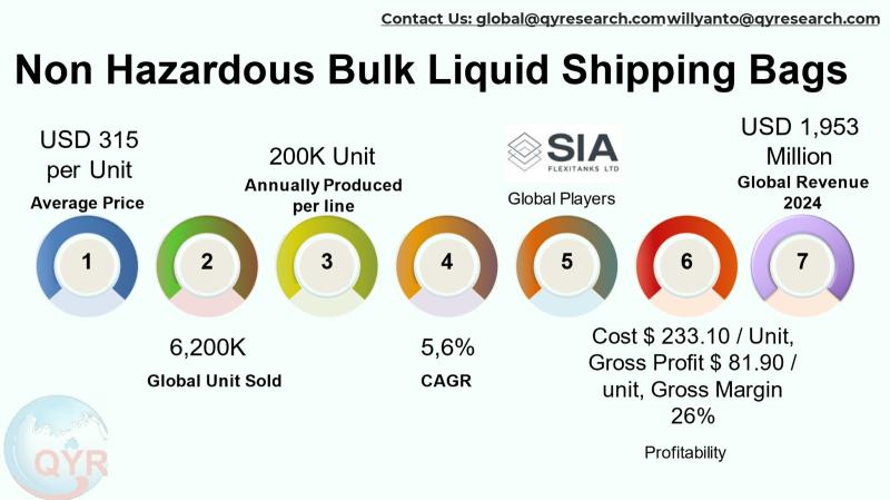
Non Hazardous Bulk Liquid Shipping Bag Market to Reach USD 2,835 Million by 2031 …
This report examines the global market for non-hazardous bulk liquid shipping bags (commonly called flexitanks or container liners) with a particular focus on Asia and Southeast Asia. These large, flexible bladders are fitted inside standard freight containers to move non-hazardous liquids such as edible oils, juices, liquid food ingredients, industrial oils, and many commodity chemicals. The technology replaces multiple drums, IBCs or small totes by converting one 20-ft container into…
More Releases for Wafer
Semiconductor Wafer Electrostatic Chucks for 300mm Wafer Market Size, Trends & F …
Semiconductor Wafer Electrostatic Chucks for 300mm Wafer Market Size
The global Semiconductor Wafer Electrostatic Chucks for 300mm Wafer market is projected to grow from US$ 1227 million in 2024 to US$ 1672.7 million by 2030, at a Compound Annual Growth Rate (CAGR) of 5.3% during the forecast period.
Get Free Sample: https://reports.valuates.com/request/sample/QYRE-Auto-38F13137/Global_Semiconductor_Wafer_Electrostatic_Chucks_for_300mm_Wafer_Market_Research_Report_2023?utm_source=openpr&utm_medium=referral
The US & Canada market for Semiconductor Wafer Electrostatic Chucks for 300mm Wafer is estimated to increase from $ million in…
Wafer Hybrid Bonding Equipment Market Share Driven by Wafer-to-Wafer Technology …
Wafer Hybrid Bonding Equipment Market Size
The global market for Wafer Hybrid Bonding Equipment was valued at US$ 164 million in the year 2024 and is projected to reach a revised size of US$ 756 million by 2031, growing at a CAGR of 24.7% during the forecast period.
View sample report
https://reports.valuates.com/request/sample/QYRE-Auto-31W14822/Global_Wafer_Hybrid_Bonding_Equipment_Market_Insights_Forecast_to_2029
The Wafer Hybrid Bonding Equipment market is experiencing accelerated growth, driven by increasing demand for advanced semiconductor packaging technologies that enable higher…
Wafer Sorting Equipment Market
The "Wafer Sorting Equipment Market" is expected to reach USD xx.x billion by 2031, indicating a compound annual growth rate (CAGR) of xx.x percent from 2024 to 2031. The market was valued at USD xx.x billion In 2023.
Growing Demand and Growth Potential in the Global Wafer Sorting Equipment Market, 2024-2031
Verified Market Research's most recent report, "Wafer Sorting Equipment Market: Global Industry Trends, Share, Size, Growth, Opportunity and Forecast 2023-2030," provides…
Semiconductor Wafer Electrostatic Chucks for 300mm Wafer Market
Semiconductor Wafer Electrostatic Chucks for 300mm Wafer Market
The global Semiconductor Wafer Electrostatic Chucks for 300mm Wafer market was valued at US$ 1165 million in 2023 and is anticipated to reach US$ 1672.7 million by 2030, witnessing a CAGR of 5.3% during the forecast period 2024-2030.
View Sample Report
https://reports.valuates.com/request/sample/QYRE-Auto-38F13137/Global_Semiconductor_Wafer_Electrostatic_Chucks_for_300mm_Wafer_Market_Research_Report_2023
Report Scope
The Semiconductor Wafer Electrostatic Chucks for 300mm Wafer market size, estimations, and forecasts are provided in terms of output/shipments (Units) and revenue…
Automatic Mounter Wafer Equipment Market Report 2018: Segmentation by Type (100 …
Global Automatic Mounter Wafer Equipment market research report provides company profile for Lintec Corporation, Nitto Denko, Tokyo Electron, Technovision, Takatori, Ultron Systems, DISCO Corp., Syagrus Systems, Advanced Dicing Technologies, Longhill Industries and Others.
This market study includes data about consumer perspective, comprehensive analysis, statistics, market share, company performances (Stocks), historical analysis 2012 to 2017, market forecast 2018 to 2025 in terms of volume, revenue, YOY growth rate, and CAGR for…
EMEA Solar Wafer Cutting Fluid PEG Market For Semiconductor, Solar Wafer, Crysta …
Latest industry research report on: EMEA (Europe, Middle East and Africa) Solar Wafer Cutting Fluid PEG Market : Industry Size, Share, Research, Reviews, Analysis, Strategies, Demand, Growth, Segmentation, Parameters, Forecasts
Request For Sample Report @ https://www.marketresearchreports.biz/sample/sample/1194694
Geographically, this report split EMEA into Europe, the Middle East and Africa, With sales (K MT), revenue (Million USD), market share and growth rate of Solar Wafer Cutting Fluid PEG for these regions, from 2012 to…
